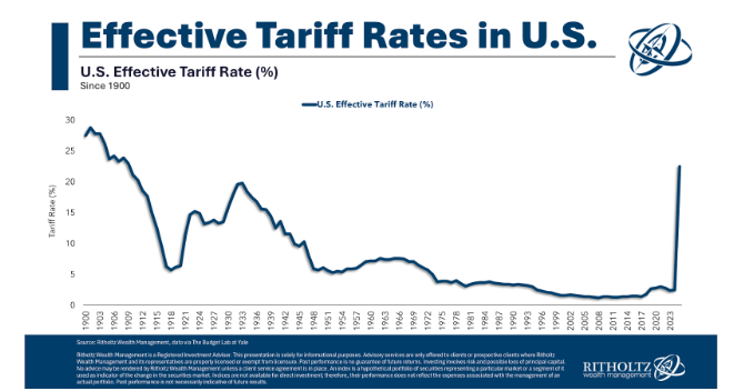


Chinese semiconductor industry gears up for domestic HBM3 production by the end of 2026 — CXMT to produce chips, while Naura, Maxwell, and U-Preseason design tools for assembly
ChangXin Memory Technologies (CXMT), the leader of the Chinese DRAM industry, is on track to build 3rd Generation high bandwidth memory (HBM3), according to Chosun Biz. Moreover, China-based Naura Technology, Maxwell, and U-Preseason are developing domestic tools specifically designed to assemble HBM memory stacks. If true, this means that in several years, China will have fully localized the production of HBM, which is crucial in the race to produce high-end AI accelerators, with Chinese companies under pressure to utilize homegrown silicon.
Built in China
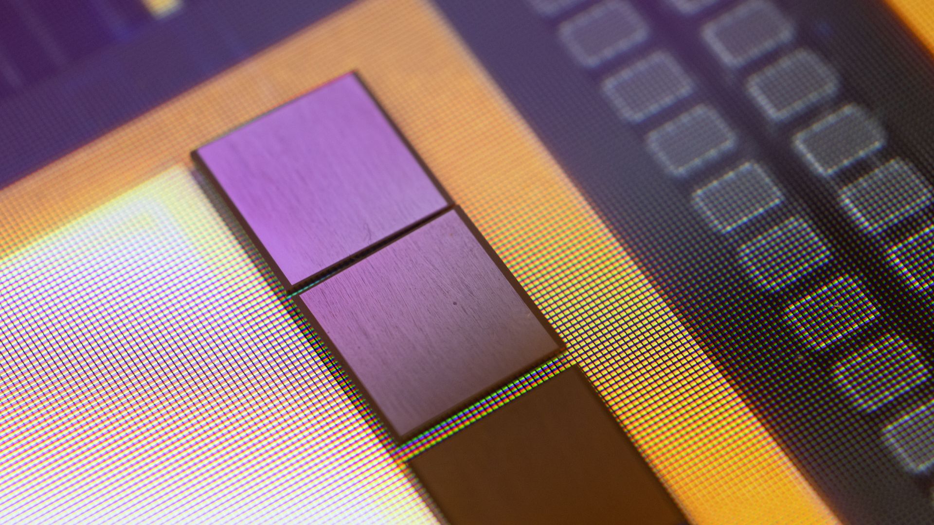
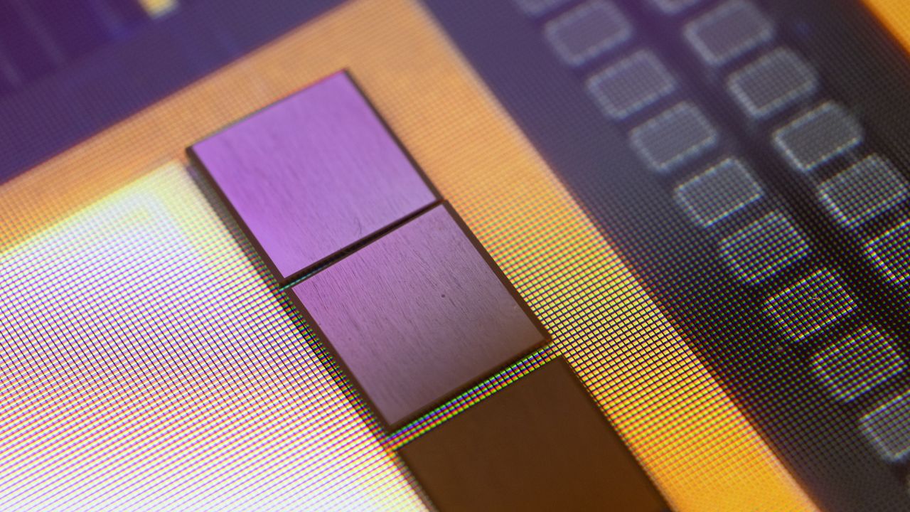
For CXMT, HBM3 is a strategically important product for many reasons. First up, HBM is significantly more expensive than the ‘commodity' DRAM that CXMT has produced so far, so entering a new market will affect CXMT's bottom line. Secondly, the availability of high-performance HBM3 is strategically important for China's AI sector. Thirdly, producing HBM3 stacks — that consist of eight or more large DRAMs with a wide I/O — will prove that CXMT is a world-class memory maker on par with Micron, Samsung, and SK hynix. Last but not least, making large HBM3 DRAM devices — which are three or four times larger than commodity DDR5 or LPDDR5 — consumes a lot of capacity. If CXMT manages to produce HBM3 in high volumes, it will need to demonstrate that it has enough capacity to address all segments of the market.
CXMT is not the only company in China to be working on HBM projects. Around two years ago Wuhan Xinxin Semiconductor Manufacturing (XMC), a foundry controlled by Yangtze Memory Technology Co. (YMTC), China's leading maker of 3D NAND, initiated a project to develop its own HBM packaging technologies using hybrid bonding and other IP from YMTC, and bought the appropriate equipment to reach a monthly production capacity of around 3,000 wafers.
XMC is also still working on its through-silicon via (TSV) process technology used in HBM, according to the report, but precise details, such as the exact development stages, remain unclear. Once XMC is done with development, it can offer integration services to DRAM makers or other interested parties.
Still, while a significant number of HBM characteristics — including performance efficiency and thermals — depend on packaging and hybrid-bond quality, XMC/YMTC will still need special HBM DRAM chips, which they will only be able to get from DRAM suppliers. We are not aware whether Chinese entities can access HBM DRAM ICs from foreign companies. If they cannot, then XMC/YMTC will have to assemble HBM modules based on memory devices made in China by companies like CXMT.
The U.S. export controls already limit multiple types of lithography and deposition tools to Chinese entities, with severely limited access to the advanced manufacturing tools required for the development and production of HBM. Consequently, China's HBM ambitions increasingly hinge on the rapid localization of etching, TSV, bonding, and packaging equipment rather than on memory design alone.
Given the limited amount of time that China may have before export limitations take place, local chipmakers must use what they have at hand while also preparing to use domestically developed tools. Chinese companies are working hard to develop and deploy their own tools required for HBM assembly; however, there is currently no indication of how ready the aforementioned tools might be for mass production.
Naura Technology, which is a leading supplier of etching equipment and currently commands 30% of the etching tools market in China, has expanded its portfolio specifically for HBM manufacturing by adapting and developing tools across multiple process steps, according to Chosun.
The company reportedly now offers not only etching systems, but also deposition systems for forming thin films on wafer surfaces, and cleaning tools optimized for HBM. These tools can be used to etch TSV structures in HBM DRAM dies, deposit liner and dielectric films required for TSV formation, and prepare wafers for subsequent bonding and other packaging steps. However, it's unclear whether these have been fully qualified and inserted into the mass production flows by companies like CXMT.
Maxwell Semiconductor has also reportedly developed next-generation hybrid bonding equipment designed to electrically and mechanically join multiple DRAM dies into a single HBM stack. Hybrid bonding is a key enabler for advanced HBM packaging as it enables ultra-fine-pitch copper-to-copper interconnects between dies and is therefore responsible for interconnect density and signal integrity.
U-Precision is another China-based WFE maker that offers equipment for HBM packaging, but it is unclear what exactly the company has to offer and whether it supplies its tools for HBM commercially.
Chinese HBM3 production likely by 2027
Based on media reports from China, there are multiple DRAM makers, chip packaging houses, and material suppliers working on developing and building HBM memory in the country. There are also wafer fab equipment makers that are either working on tools for HBM assembly itself or are already shipping them.
Keeping in mind the rapid progress that China's semiconductor industry has made in the last 20 years, we have little doubt that companies like CXMT and XMC/YMTC can establish volume production of HBM3 memory in 2026 ~ 2027.
However, even if CXMT and its peers can produce suitable DRAM dies, their HBM supply could be limited by back-end throughput and yield, specifically stacking/assembly, bonding, warpage, and slow overall package yield learning curves, as HBM3 is a new technology for CXMT. If Chinese memory makers start to use all-new equipment from local suppliers, their yield ramp could be even slower, especially if manufacturers lack proper inspection and testing tools.
The biggest challenge with ramping HBM is not production of large DRAM dies, stacking them on the base die, or even interconnecting them; it is the combination of these steps, where a single misstep ruins the whole package, and therefore the economy behind it. For now, China has no choice but to continue working on its HBM supply, but it may take years before it manages to saturate its own market with HBM, as this type of memory is inherently more difficult to produce than commodity DRAM like DDR5 or LPDDR5.